
PCB: What is it and Why are they so Important in Electronic Devices
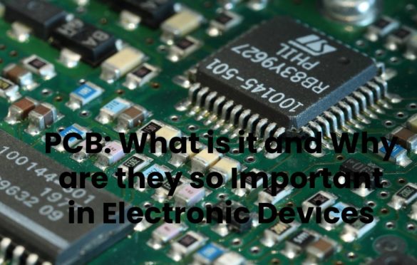
Regardless of their aggressive, military or minimalist appearance, motherboards are the essential element of our computers, but do we know everything we need about them? The different lines on our motherboard that look like cables are the printed circuit connections on the board. Printed Circuit Boards (PCBs) are in all electronic devices today.
It spreads PCBs’ presence and cables, integrated circuits, and regulators throughout the chassis in the past. Making these PCBs a process similar to that of processors followed, although with a lower complexity level.
Table of Contents
An Elaborate Manufacturing Process that Reduces the Size of the Circuits of our Devices
Fiberglass strips are stacked and then treated with a resin to stick to each other, becoming a concrete block. Then copper is placed on both sides and covered with a photoresist chemical.
Although this, a pattern is superimposed using the lines where they want them to go on the plate. And exposed to ultraviolet light. In a little, though, as this process ends, the PCB is “cleaned,” and the copper remains in the areas wherever we make sure placed the pattern. It is how the manufacturing process begins, but let’s not forget that it is a layered structure, and the visible marks do not have to be the same on the inside – never try to add holes to a PCB yourself.
During the manufacturing process, these layers receive interconnection patterns. They also have connections to different capacitive components such as resistors or capacitors, other layers of the PCB itself, or controllers of the various input/output ports required in the electronic device. All these components will remain sold to the board, following a different process from the “wired” connections.
We have Smaller and Smaller Devices
PCBs are used to create motherboards, although they are the best example that we have been able to use to see how useful they are. They are also essential in electronic devices such as smartphones. In these devices, the process has taken even further. And they are “double-sided” PCBs where on each side of the board, here are different components. It manages to significantly reduce the space used and thus be able to make smaller devices.